Avoid damaging your PCBA board by correctly selecting sockets and test probes when designing a fixture.
The Fixtures design process at iBtest starts with direct collaboration with our client to understand their requirements and provide tailored solutions to each specific need.
Our engineers' high level of experience at iBtest enables them to respond quickly. Our close relationships with various suppliers also allow us to offer specialized attention with high-quality standards.
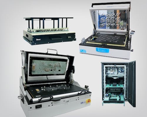
Among the solutions offered by the Fixture department at iBtest is manufacturing FCT (Functional Circuit Test) off-line Fixtures. Below, we describe the main guidelines engineers evaluate when designing a Fixture.
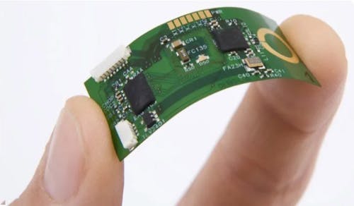
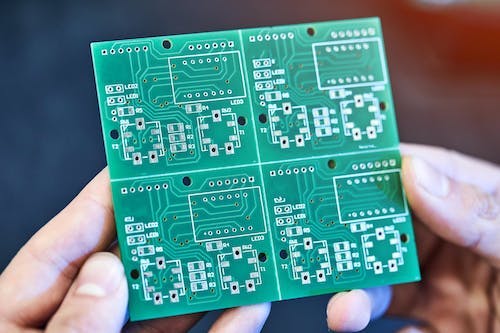
FCT Off-line Fixtures are focused on verifying the proper functioning of the components specified on the PCB (Printed Circuit Board). The design stage of FCT Off-line Fixtures begins with the appropriate selection of two fundamental parts, allowing optimal PCB testing.
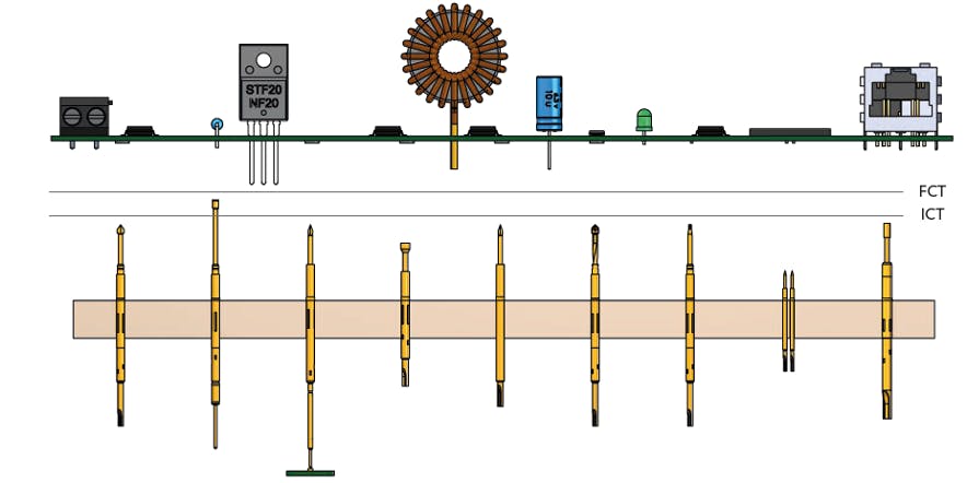
As the first parameter, we will select the type of Socket, and lastly, the type of Test Probe will be chosen.
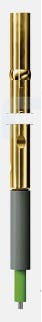
Socket (Receptacles)
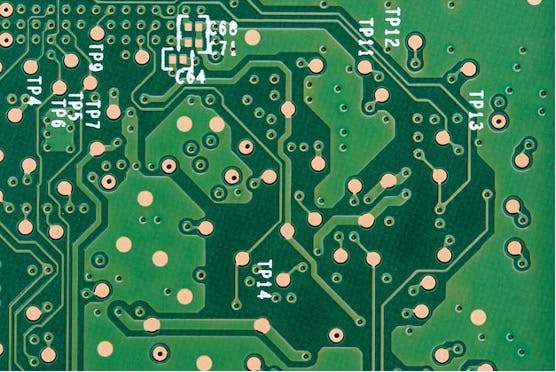
a) The spacing between the test points, as it conditions the type of Socket to use since there is a minimum distance (d) between two test points for mounting a particular Socket. The most common minimum separations between test points are:
- 40mil (1.02mm)
- 50mil (1.27mm)
- 75mil (1.91mm)
- 100mil (2.54mm)
b) The method that will be used to connect the Socket to the measurement instrument; the most common methods for connecting a socket are:
- Wire-wrap connection: They have a square termination that can be used to wrap a small gauge cable.
- Solder Cup connection: They have a small cup-shaped termination for soldering a cable.
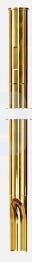
- Wired connection: They have a short cable at their termination that can be used to connect the Socket to the measurement instruments.
Test Probe
The selection of a test probe involves understanding its fundamental classification regarding the geometry of the test point to be contacted; the main types are:
a) PADs: These are flat test points on PCBs that can be contacted with aggressive and passive test probes.
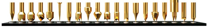
b) PINs: These are terminations of components integrated into PCBs and can be contacted with test probes that help achieve better alignment.
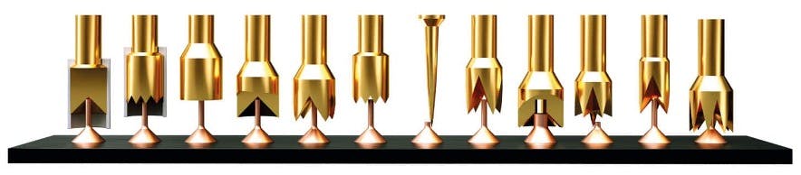
c) Posts: These are components found on a PCB, similar to PINs; hence, it is also appropriate to use self-centering test probes.
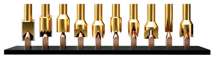
d) Vias: Designated as the vertical contact that goes through the layers of a PCB. VIAs can be contacted using the sharp edges of the head shapes on the inner ring of the connection that goes through the layers or with a crown tip on the front surface of the VIA.
The correct selection of the parameters mentioned above allows for the customization of the design according to the requirements and needs of each client.